
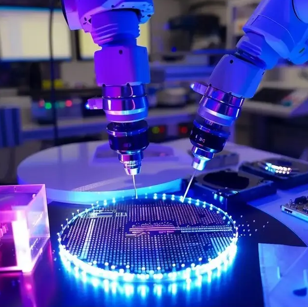
Getting Lead-Free Curing Right with Infrared
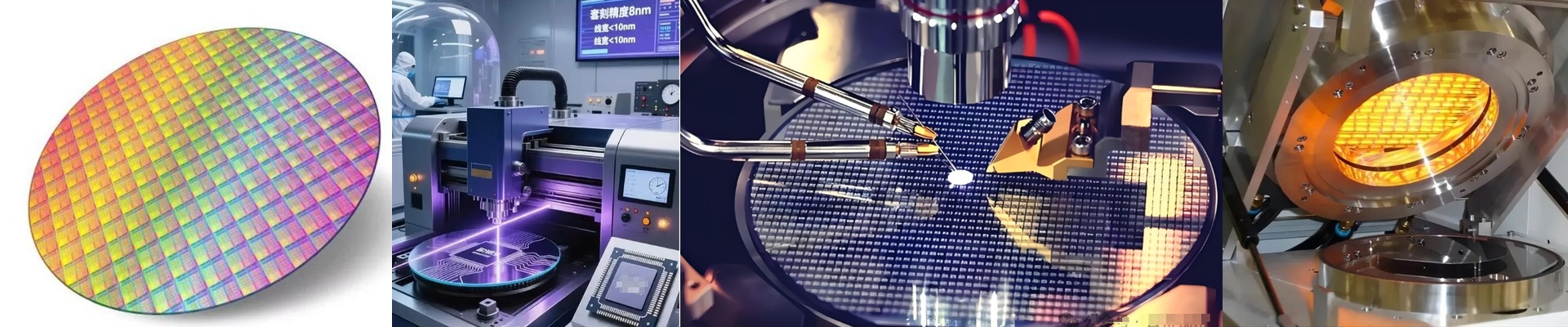
The industry is pushing hard toward “green” and lead-free standards for semiconductor drying. Honestly, it’s about time. We’ve moved over to infrared (IR) curing because it lets us ditch the nasty chemical solvents and heavy-metal catalysts you usually find in those old-school ovens.
How the heat actually works
Think about a standard convection heater. It wastes so much time just warming up the air around the part. IR is different. It uses electromagnetic radiation to send energy straight into the substrate. We tune these systems to hit the specific absorption bands of your coating or adhesive.**You’re heating the part, not the air.**That’s why your power bill drops—you aren’t spending kilowatts just to make a big metal box hot.
The build: Stainless steel and shielding
Since we’re talking about clean-room environments, we can’t have random flakes of rust landing on a silicon wafer. That’s why we build the housings from high-grade stainless steel. It stays clean. Plus, the interior is designed to bounce those IR waves right back toward the target to keep the heat dense. One quick tip: make sure your grounding is spot on. These high-wattage arrays can kick out a lot of EMI if your shielding isn’t tight. It’s a small detail that causes a huge headache if you miss it.
The catch (and how to handle it)
IR is fast. Like, “hours-turned-into-seconds” fast. But that speed comes with a risk. If you crank the power too quickly, you get a nasty thermal gradient. You might warp the substrate or deal with “skinning,” where the top layer cures and traps solvents underneath. It’s a balancing act between your wattage and your belt speed. We designed these to be drop-in replacements for those clunky legacy convection tunnels. You get a smaller footprint and lower costs, as long as your cooling system can keep up with the concentrated heat.